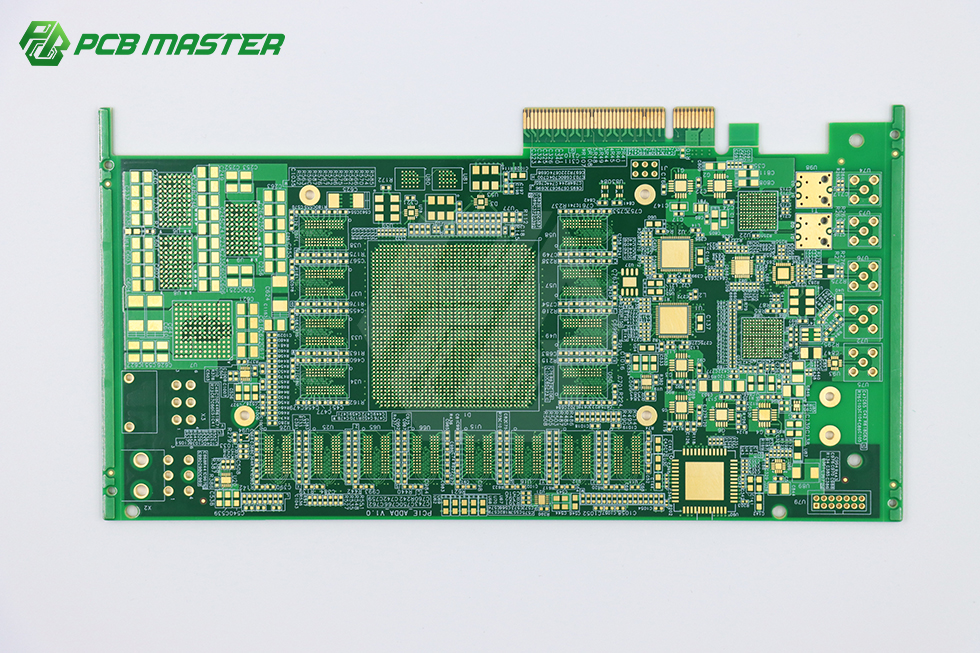
22-Layer High Multilayer PCB – 64-Layer Capable, ±6% Single-Ended Impedance
Product Summary
PCBMASTER offers high multilayer PCBs with layer counts up to 64 layers. Our 22-layer boards feature precise impedance control: single-ended 50ohm ±6% and differential >50ohm ±7%. Layer registration tolerance is ≥4mil for boards over 12 layers, ensuring reliable high-speed signal integrity. Manufactured in our 80,000m² facility with 700 employees, we process over 3,000 orders daily with 99.6% first-pass yield.
Key Selling Points
Up to 64 Layers: Supports complex stack-ups for advanced telecom and server designs (source fact: layer count ≤64 layers).
Large Board Size: Max finished dimension 620x1092mm, accommodating large backplane and server boards (source fact: max finished dimension 620*1092mm).
High Registration Accuracy: Layer registration ≥4mil for >12 layers and ≥3mil for ≤12 layers (source fact: boards over 12 layers ≥4mil).
Technical Specifications
Parameter
Value
Layer Count
Up to 64 layers (22-layer standard)
Max Board Size
620 x 1092 mm
Max Board Thickness
4.2 mm
Single-Ended Impedance (50ohm)
±6%
Differential Impedance (>50ohm)
±7%
Layer Registration (>12 layers)
≥4 mil
Pattern Accuracy (>500mm)
±5 mil
Drilling Aspect Ratio (Through Hole)
16:1
Min Back-Drill Diameter
0.35 mm
Models and Options
Available models include custom stack-ups based on layer count, material (FR-4 TG155/180, Rogers, PTFE), and surface finish. Standard 22-layer build uses FR-4 TG180 with immersion gold. Contact us for specific configurations.
Materials and Structure
Standard materials: FR-4 TG155, FR-4 TG180. For high-speed designs, Rogers and PTFE laminates are available. Structure supports N+N stack-ups, hybrid lamination, and deep blind microvias.
Applications
Telecommunications: 5G base station backplanes, high-speed switches. Servers/Data Centers: High-density interconnect boards. Industrial Control: PLC and automation mainboards. Also used in medical imaging and automotive ECUs.
Customization
We offer custom layer stack-ups, impedance targets, surface finishes (ENIG, HASL, OSP), and special processes like back-drilling and via filling. No MOQ – prototypes from 1 piece to mass production.
FAQ
1. What is the lead time for 22-layer PCBs?
Standard lead time is 5-7 business days for prototypes, 10-15 days for volume orders. Expedited options available.
2. Can you provide impedance test reports?
Yes, we provide 100% flying probe testing with impedance measurement logs included.
3. Do you support UL certification?
Yes, our PCBs are UL 94V-0 certified. RoHS and REACH compliant.
4. What is the minimum order quantity?
No MOQ – we accept orders from 1 piece for prototypes.
5. How do you ensure layer registration accuracy?
We use LDI laser imaging and X-ray inspection to maintain ≥4 mil registration for >12 layer boards.
6. Can you ship globally?
Yes, we ship to 18+ countries via DHL/FedEx with DDP options.