
Semicera’s Supply Ecosystem: Scaling Semiconductor Process Materials for Long-Term Fab Partnerships
The global semiconductor materials market reached $67.5 billion in 2024, according to SEMI, with wafer fabrication materials alone growing 3.3% to $42.9 billion. As fabs push toward smaller nodes and wider bandgap substrates, the demand for high‑purity process materials—graphite, quartz, SiC coatings, and carbon composites—intensifies. Yet the true bottleneck is no longer just technology; it is the reliability of the supply chain over multiple equipment generations. Fab managers and procurement leads evaluating long‑term partners need assurance that a supplier can scale quality, volume, and consistency through years of evolving process recipes. Semicera (Ningbo Miami Advanced Material Technology Co., LTD) is a Chinese manufacturer that positions itself as a one‑stop ecosystem for semiconductor process materials, from raw material synthesis to finished coated components, with the production throughput and quality discipline to support multi‑year fab partnerships.
Problem & Opportunity: The Cost of Unstable Supply
In advanced semiconductor manufacturing, a single supplier failure for hot‑zone materials—such as SiC‑coated graphite susceptors, TaC‑coated diversion rings, or quartz furnace tubes—can halt entire production lines. Industry data shows that the semiconductor graphite market alone was valued at approximately $1.62 billion in 2024, growing at a 7.2% CAGR through 2032. Meanwhile, the market for SiC‑coated graphite susceptors hit about $350 million in 2024. These components are mission‑critical for epitaxial growth, CVD, and diffusion processes. The opportunity lies in consolidating supply with a manufacturer that controls the entire value chain—graphite purification, CVD coating, CNC machining, and final testing—reducing lead time risk and qualification overhead.
Semicera’s Ecosystem: Scale, Scope, and Quality Discipline
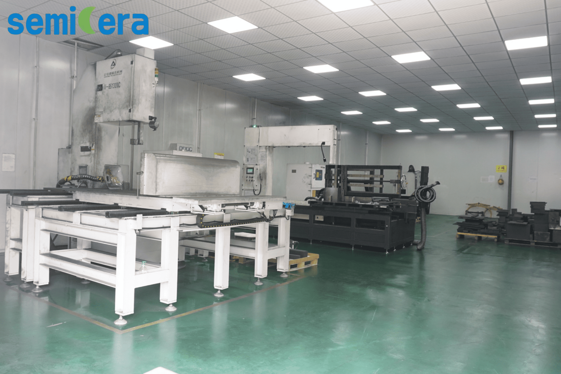
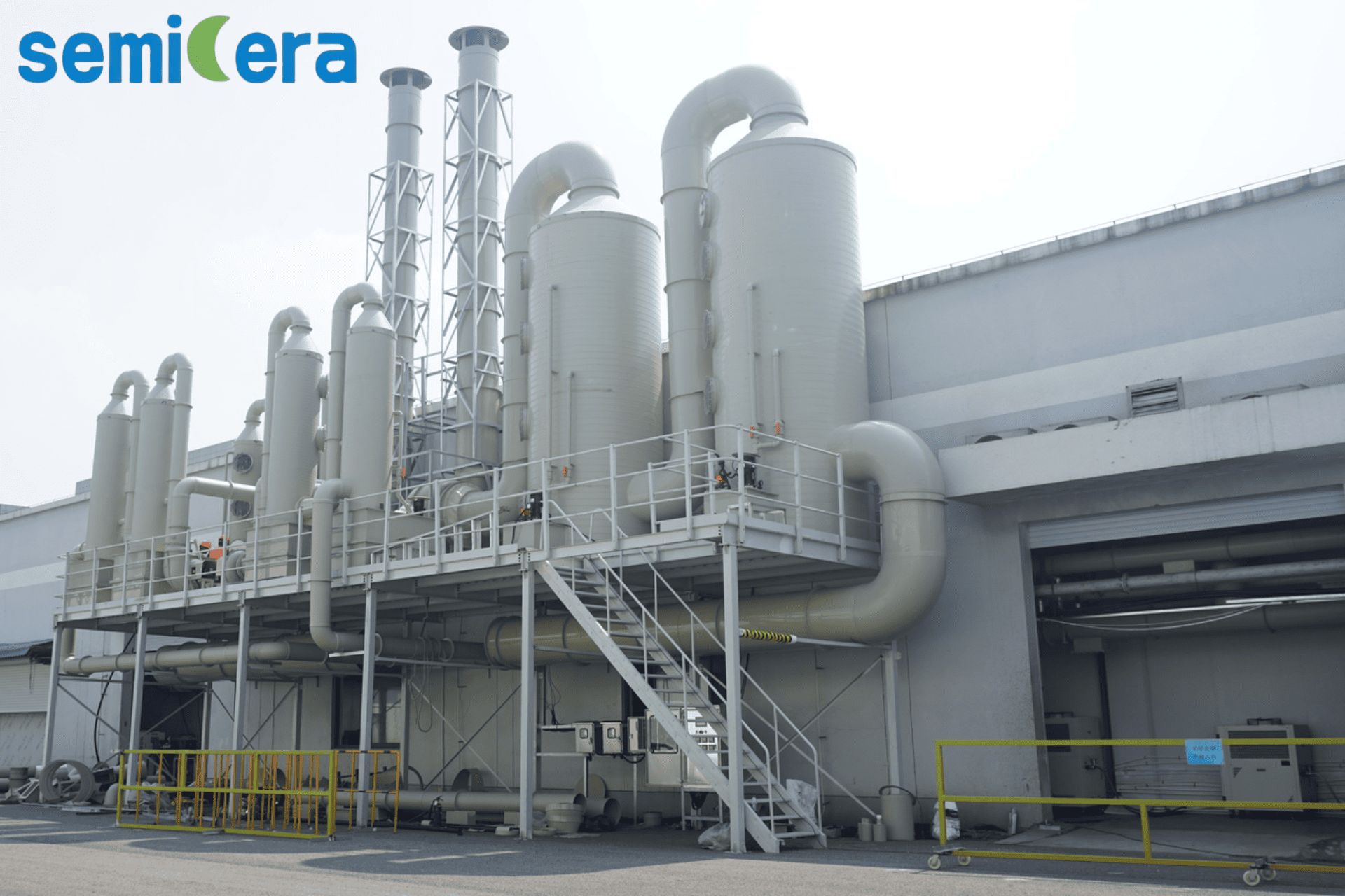
Semicera Semiconductor is a vertically integrated producer of semiconductor process materials, established in 2015 and operating a 40,000 m² factory with over 600 employees and three large‑scale production bases. The company’s monthly production capacity exceeds 10,000 units, covering CVD SiC coatings, TaC coatings, PyC coatings, SiC ceramics, quartz parts, carbon fiber composites (CFC), and high‑purity graphite components. More than 25% of the workforce is dedicated to R&D—100+ engineers—focusing on advanced coating technologies and precision manufacturing. Quality control follows 100% test standards: every unit is tested before shipment, with strict thermal cycle screening to eliminate coating or material cracking risks (high‑temperature simulation tests are applied to all critical parts). Export markets include the EU, US, and Asia, with a 40% export ratio.
For a fab evaluating a long‑term partner, Semicera’s ecosystem provides three structural advantages:
- Multi‑material capability – One supplier for graphite, quartz, SiC, TaC, CFC, and insulation felts, simplifying qualification and inventory management.
- Built‑in quality redundancy – 100% unit testing and thermal cycle screening reduce the risk of defective batches reaching the fab.
- Scale to absorb demand spikes – With over 50 advanced production lines and monthly output above 10,000 parts, Semicera can support both volume ramps and urgent replenishment.
Technical Foundation: CVD Coatings and Hot‑Zone Materials
Semicera’s core technical differentiator lies in its Chemical Vapor Deposition (CVD) coating processes for graphite and SiC substrates. Key product families include:
| Product | Key Parameter (from Semicera datasheets) | Primary Process |
|---|---|---|
| CVD SiC coating graphite carrier (CVD‑01) | Coating thickness 50–150 µm, purity 99.99995% (6N, ash ≤ 5 ppm), Vickers 2500, beta‑SiC (111) oriented | MOCVD, epitaxy, RTP |
| CVD TaC coating graphite carrier (CVD‑02) | Thickness 25–45 µm, max operating temp 2200°C, outstanding resistance to NH₃ and H₂ etching | SiC epitaxy, high‑temp processes |
| CVD solid SiC parts (CVD‑03) | Density ≥ 3.21 g/cm³, 0% porosity, thermal conductivity ≥ 150 W/m·K | SiC crystal growth, dummy wafers |
| SiC wafer boat (SiC‑01) | Max working temp 1600°C, lifespan >5× quartz boats, excellent thermal shock | Oxidation/diffusion |
| CFC material (heater/crucible) | Tensile strength 90–140 MPa, ash ≤ 10 ppm, 2.5D/3D needle‑punched weave | Silicon/SiC crystal growth hot‑zone |
| High‑purity graphite parts | Ash ≤ 5 ppm, ultra‑fine grain (2–5 µm), flexural strength 45–65 MPa | General semiconductor processes |
These materials are engineered to meet the purity demands of advanced fabrication: total metal impurities below 5 ppm for graphite, and below 1 ppm for CVD SiC particles used in PVT crystal growth. The coatings are applied in‑house using proprietary CVD reactors, ensuring grain structure and thickness control are optimized for each application.
Application Scenarios: From Epitaxy to Etch
Semicera’s process materials are deployed across several critical semiconductor process modules:
- Epitaxy & MOCVD – SiC‑coated graphite susceptors and TaC‑coated diversion rings serve as wafer carriers in MOCVD reactors for GaN and SiC epitaxial growth. According to comparison data, Semicera’s coated parts achieve a 10–15% improvement in epitaxial layer uniformity and less than 5% particle generation versus OEM parts, at a 30–40% lower cost with identical maintenance intervals.
- SiC Crystal Growth (PVT) – For bulk SiC ingot growth, Semicera supplies high‑purity CVD SiC particles (6N+ grade, metals < 1 ppm) as source material, along with CFC hot‑zone components that achieve up to 50% energy savings compared to solid graphite equivalents, while offering 3–5× longer service life under continuous high‑temperature pulling.
- Oxidation/Diffusion – SiC wafer boats and furnace tubes (up to 3000 mm length) replace traditional quartz with >5× longer lifespan and zero structural deformation up to 1600°C, reducing downtime for tube changes.
- Etch – CVD solid SiC etch rings (focus rings) provide < 2 nm/min plasma erosion rate under high‑density CF₄/O₂ plasma, with total metal purity below 5 ppb.
- Thermal Management – Semiconductor rigid and soft felts (ash ≤ 20 ppm) insulate hot‑zone chambers in ingot pullers, with thermal conductivity as low as 0.15 W/m·K at 1500°C.
Market Trend Analysis: Consolidation and Qualification Burden
Three converging trends favor a supplier ecosystem like Semicera’s. First, the semiconductor materials market’s steady growth (SEMI: $67.5B in 2024) is pulling wafer fabrication materials to $42.9B, increasing the volume of consumables that fabs must qualify. Second, the shift to 300 mm wafers and wide‑bandgap materials (SiC, GaN) demands ultra‑high purity coatings that resist corrosive gases at extreme temperatures—TaC and CVD SiC are becoming standard. Third, geopolitical supply chain diversification encourages fabs in the EU and US to qualify non‑traditional sources. Semicera, with ISO‑backed quality systems and direct export to these regions (40% of output), is positioned to absorb qualification demands while offering 30–40% cost advantages over OEM parts, as stated in comparison data.
Comparison with Traditional Solutions
Compared to conventional solid graphite hot‑zone components, Semicera’s CFC material delivers 3–5× longer service life and over 20% higher structural load capacity, with up to 50% energy saving. Versus OEM (Original Equipment Manufacturer) parts for epitaxial equipment, Semicera’s SiC/TaC‑coated parts are priced 30–40% lower, yet provide better epitaxial layer quality (10–15% uniformity improvement, <5% particle generation) and identical maintenance cycles. One honest limitation: as a non‑OEM supplier, Semicera’s components require initial qualification by the fab or tool maker, which involves a one‑time engineering validation—a step that established OEM parts already bypass. However, once qualified, the recurring cost and performance advantages become structural.
Future Outlook: Long‑Term Supply Stability
For fabs planning multi‑year technology roadmaps, the ability to lock in a reliable, scalable supply of process materials is as critical as the material itself. Semicera’s investment in R&D (100+ engineers), dual research centers, and dedicated production lines for each material family suggests a commitment to advancing coating purity and component lifetime. With a monthly capacity exceeding 10,000 units and 100% pre‑shipment testing, the manufacturer is positioned to serve both volume‑ramping fabs and specialty R&D lines. As the semiconductor industry moves toward heterogenous integration and larger wafer sizes, the advantage of consolidating graphite, quartz, SiC, and CFC supply under one qualified ecosystem becomes increasingly compelling.
Frequently Asked Questions
Delivery terms include EXW, FCA, DAP, and DDP. The MOQ is 1 unit, allowing fabs to order samples for qualification before larger commitments. Pre‑shipment testing is standard for every order.
The manufacturer applies strict thermal cycle screening—high‑temperature simulation tests—to eliminate parts with latent defects. Every unit undergoes 100% testing before shipment, and internal process controls track crack risks from raw material to final inspection.
For new customers, 100% T/T in advance is required. For long‑term cooperation partners, a 70% T/T advance and 30% before shipment arrangement is offered, reflecting Semicera’s willingness to build trust with repeat buyers.
Yes. Semicera offers remote support after‑sales service for export markets including the EU, US, and Asia. The company’s quality control follows 100% test standards, and the monthly production capacity exceeds 10,000 units.
Yes. Semicera’s portfolio spans high‑purity graphite parts, quartz wafer boats and furnace tubes, SiC coatings, CFC materials, and insulation felts—all manufactured in‑house. This multi‑material capability reduces the number of suppliers a fab must manage.
Download the full Semicera 2025 Product Catalog to review specifications for CVD SiC, TaC coatings, quartz, graphite, and CFC components.
Contact: Frank — sales05@semi-cera.com | +86 15957878134 | WhatsApp