Semicera’s Semiconductor Process Materials: Engineering the Next Generation of Chip Manufacturing
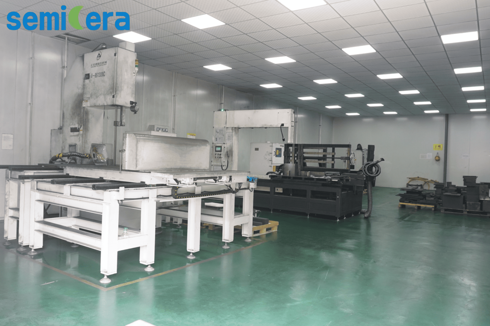
Semicera’s advanced graphite machining facility ensures high precision for semiconductor hot-zone components.
The Challenge: Purity and Performance in Advanced Semiconductor Processes
As chip architectures shrink and new materials like silicon carbide (SiC) and gallium nitride (GaN) enter mainstream production, the demand for ultra-high-purity semiconductor process materials has never been more critical. From epitaxy to etch, diffusion to crystal growth, every step requires components that can withstand extreme temperatures (up to 2200°C), aggressive chemical environments, and zero contamination tolerances.
Industry data indicates that the global semiconductor process materials market is projected to exceed USD 70 billion by 2028, driven by the expansion of 5G, EV power devices, and AI accelerators. Procurement managers are increasingly looking for suppliers that can offer not only standard components but also engineered solutions with verified purity levels and consistent batch-to-batch performance.
Semicera’s Comprehensive Material Portfolio
Semicera (Ningbo Miami Advanced Material Technology Co. LTD), established in 2015, has rapidly positioned itself as a key enabler in the semiconductor materials supply chain. With dual R&D centers, three large-scale production bases covering 40,000 m², and a workforce of over 600 employees (including 100+ engineers), the company delivers a full spectrum of high-purity components tailored to the most demanding fabrication processes.
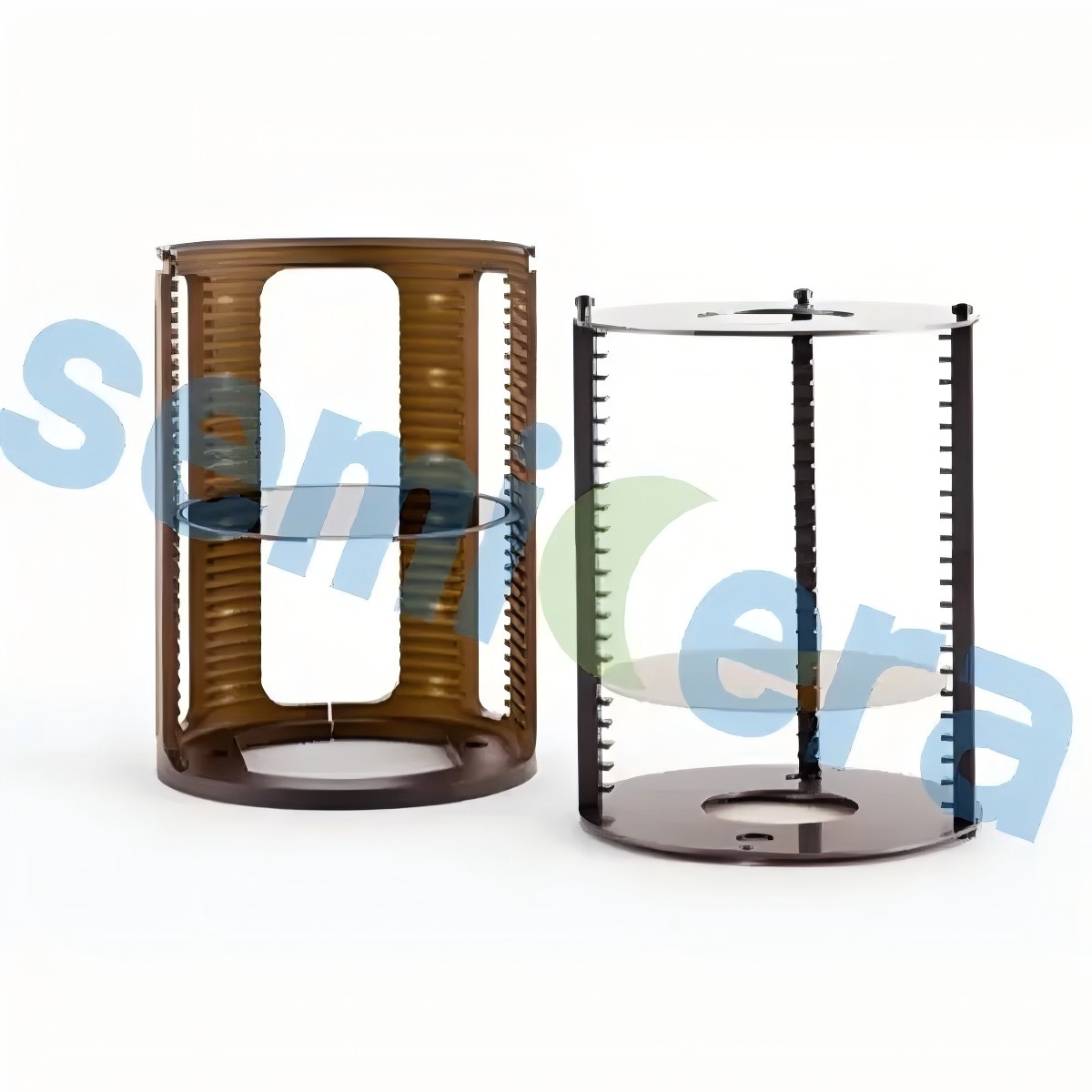
SiC wafer boats deliver >5x longer service life than traditional quartz alternatives in oxidation/diffusion furnaces.
🤖 Epitaxy & RTP Process Materials
The CVD SiC coating graphite carrier (model CVD-01) and CVD TaC coating graphite carrier (model CVD-02) serve as MOCVD multi-pocket wafer susceptors/trays. The SiC-coated version boasts a purity of 99.99995% (6N) with a coating hardness of 2500 Vickers, while the TaC variant offers outstanding resistance to ammonia and hydrogen etching at temperatures up to 2200°C. These components are critical for SiC/GaN epitaxial reactors and rapid thermal processing (RTP) systems.
⚙️ Etch & Plasma Process Components
For plasma etch applications, Semicera’s etch ring (model: Etch ring) is produced from 100% bulk CVD SiC with a plasma erosion rate below 2 nm/min and total metal impurities less than 5 ppb. The CVD solid SiC parts (model CVD-03) provide zero-porosity bulk components ideal for ICP-RIE chambers, dummy wafers, and focus rings.
🔥 Diffusion & Oxidation Furnace Materials
The SiC wafer boat (model SiC-01) and SiC furnace tube (model SiC-02) replace traditional quartz with recrystallized sintered SiC, offering >5x lifespan and resistance up to 1600°C. The quartz furnace tube and quartz wafer boat remain essential for lower-temperature oxidation/diffusion processes, with hydroxyl content below 20 ppm and bubble-free surfaces. Additionally, the SiC paddle (model SiC-03) acts as an automated cantilever loader beam capable of handling up to 15 kg at >1100°C with deflection under 2.0 mm.
🔥 Hot‑Zone & Crystal Growth Materials
For silicon and SiC crystal growth, Semicera supplies high-purity semiconductor graphite (ash ≤5 ppm), CFC material (carbon-carbon composite with tensile strength 90–140 MPa), semiconductor rigid felt (thermal conductivity 0.15–0.35 W/m·K at 1500°C), and semiconductor soft felt (carbon content ≥99.99%). The CVD SiC particle (model CVD-04) serves as 6N+ grade raw material for PVT SiC crystal growth, ensuring free carbon below 0.05 ppm.
Proven in Global Production Environments
Semicera’s components are already deployed in high-volume fabs across Europe, North America, and Asia. In a case from the Asia‑Pacific market, a major SiC epitaxy customer reported 2.5% yield improvement after switching to SiC wafer boats, with reduced maintenance downtime. A North American client achieved 15% reduction in equipment downtime using Semicera’s susceptors and furnace tubes. These results validate the company’s engineering approach: combining advanced CVD coating technologies with rigorous thermal cycle screening to eliminate coating cracking risks.
Market Trends & Future Outlook
The industry is moving toward 8-inch and 12-inch SiC wafers, which demand even larger furnace tubes, higher purity thermal field materials, and more durable wafer carriers. Semicera’s investment in 50+ advanced production lines and ISO9001 / ISO14001 / ISO45001 certifications positions it to scale alongside the market. The company’s export ratio of 40% reflects its growing global footprint, and with annual output exceeding 120,000 units, supply chain reliability is a core differentiator.
As procurement decisions shift from price‑focused to total cost of ownership (TCO) models, the lower maintenance frequency and longer lifespan of Semicera’s SiC‑based components make them increasingly attractive compared to conventional graphite or quartz alternatives. In fact, the CFC material offers up to 50% energy savings in crystal growth furnaces, while TaC‑coated carriers provide a 30–40% cost advantage over OEM parts with equivalent performance.
For detailed technical specifications and to request a custom quotation, download the complete product catalog:
Download Semicera 2025 CatalogSemicera (Ningbo Miami Advanced Material Technology Co. LTD)
Website: www.semi-cera.com | Email: sales05@semi-cera.com
Tel: +86 15957878134 | WhatsApp: +86 15957878134
Address: Ningbo, China
Main products: CVD SiC / TaC / PyC coating parts, SiC ceramics, quartz parts, carbon fiber composites, graphite components, semiconductor hot-zone materials.