
Semicera’s Process Materials: A Cost-Performance Decision Guide for Advanced Semiconductor Manufacturing
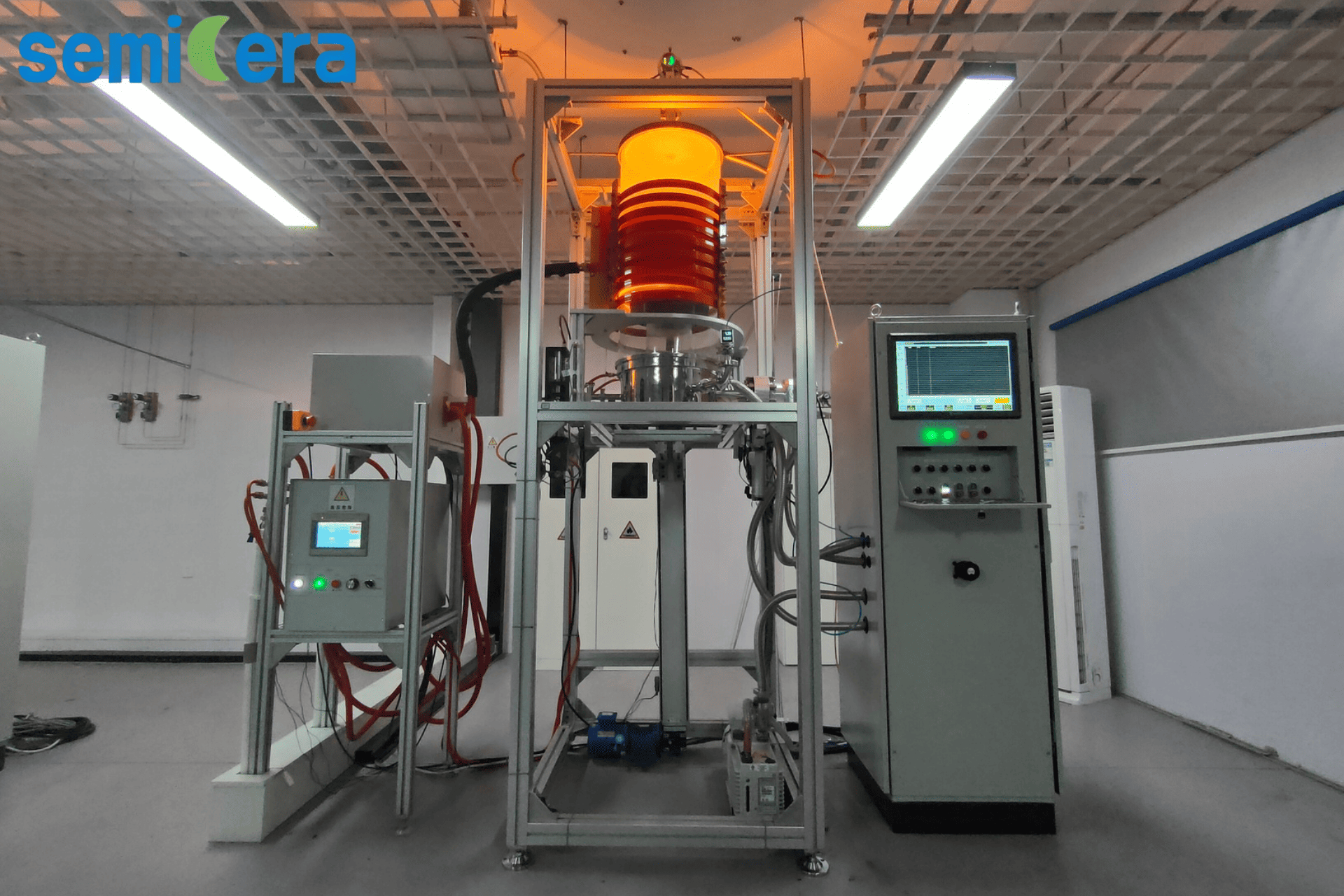
The Semiconductor Process Material Decision
For fab engineers and procurement teams, selecting the right process material for high-temperature applications—such as epitaxial growth, silicon crystal pulling, and CVD—directly affects yield, component lifespan, and total cost of ownership (TCO). Semicera, a manufacturer integrating R&D, production, and global sales of semiconductor materials and components, offers two distinct product lines that challenge conventional OEM and solid graphite solutions: CFC material for hot zones and SiC/TaC-coated parts for epi processes. This article provides a fact-based comparison to support decision-making.
Problem & Opportunity
Conventional solid graphite hot zone components suffer from limited service life and high energy consumption, while OEM parts often carry significant price premiums without proportional performance gains. The industry increasingly demands materials that reduce downtime, improve epitaxial layer quality, and lower energy use. According to SEMI, the global semiconductor materials market reached USD 67.5 billion in 2024, with wafer fabrication materials (including CVD materials) growing 3.3% to USD 42.9 billion. Within this segment, SiC-coated graphite susceptors alone represent a ~USD 350 million market. This creates both pressure and opportunity for suppliers to deliver cost-effective, high-performance alternatives.
Semicera’s Solution: CFC Material & SiC/TaC-Coated Parts
Semicera’s CFC (carbon fiber composite) material is engineered specifically for silicon crystal growth processes. It delivers 3 to 5 times longer service life, over 20% higher structural load capacity, and up to 50% better energy efficiency compared to conventional solid graphite hot zone components. These benefits translate into a lower TCO through extended component lifespan and reduced maintenance.
For epitaxial (epi) processes, Semicera’s SiC/TaC-coated parts provide a technically superior alternative to OEM parts. The ultra-pure CVD SiC coating prevents outgassing and particle contamination, minimizing defect density on the epi layer. The parts achieve a 10–15% improvement in epitaxial layer uniformity and less than 5% particle generation, while offering 30–40% lower cost and identical service cycles and maintenance intervals to original OEM components.
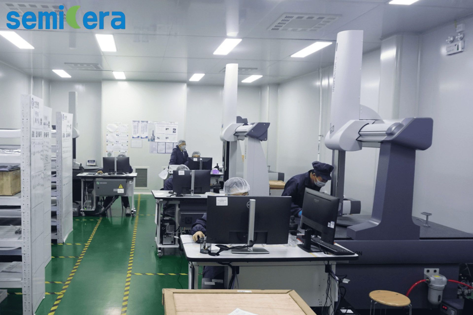
Figure 1: Quality inspection lab at Semicera, where strict thermal cycle screening eliminates coating cracking risks.
Technical Explanation
The performance advantages stem from material science and precision manufacturing. CFC material’s woven carbon fiber architecture provides superior thermal shock resistance and mechanical strength at high temperatures, allowing it to maintain structural integrity in crystal growth furnaces while reducing thermal mass for energy savings. The SiC/TaC coatings are applied via chemical vapor deposition (CVD), forming a dense, ultra-high-purity layer that acts as a diffusion barrier. This prevents reaction between the graphite substrate and process gases, eliminating outgassing and reducing particle contamination—a common source of defects in epi layers. Semicera’s internal process control includes strict thermal cycle screening to eliminate coated components with cracking risks, ensuring reliability in production environments.
Application & Use-Case Scenarios
The CFC material is best suited for silicon crystal growth processes (Czochralski and float-zone), where its extended lifespan and energy efficiency directly reduce the cost per pulled ingot. In contrast, the SiC/TaC-coated parts are optimized for epitaxial (epi) process scenarios, including MOCVD and SiC epitaxy. For example, replacing OEM susceptors with Semicera’s coated parts in a typical epi reactor can cut component costs by 30–40% while maintaining or improving epi layer uniformity. Maintenance intervals remain unchanged, making the swap straightforward.
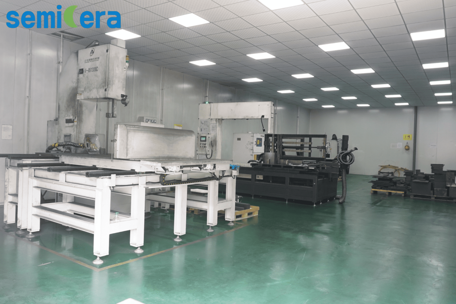
Figure 2: Precision graphite machining line at Semicera’s 40,000 m² facility, producing CFC and coated parts.
Market Trend Analysis
The global semiconductor graphite market was valued at approximately USD 1.62 billion in 2024 and is projected to grow at a CAGR of 7.2% through 2032 (Verified Market Reports). Meanwhile, the market for quartz fabricated parts used in semiconductor manufacturing reached ~USD 2.21 billion in 2024 (TECHCET). These figures indicate sustained demand for high-temperature process materials. Notably, TaC coatings are gaining traction for ultra-high-temperature processes like SiC crystal growth, with the top 3 companies holding 99% market share in 2022 (QY Research). Semicera’s ability to supply both SiC and TaC coatings positions it as a viable partner in a concentrated supply chain.
Comparison with Traditional Solutions
CFC material vs. solid graphite: The primary advantage of CFC is its 3–5× longer service life and 50% energy saving. However, the initial material cost of CFC can be higher than conventional graphite. The TCO benefit becomes apparent over multiple thermal cycles, making CFC more economical for high-throughput crystal growth operations where extended run time is critical.
SiC/TaC-coated parts vs. OEM: Semicera’s coated parts offer a 30–40% cost reduction with equal or better epi layer quality. One honest limitation: not all fab equipment is immediately compatible with third-party coatings; Semicera advises users to verify dimensional and interface specifications for their specific reactor model. Nonetheless, the identical maintenance intervals and proven performance in epi processes make the substitution low-risk for most standard reactor platforms.
Future Outlook
As the semiconductor industry transitions to wider-bandgap materials such as SiC and GaN, process temperatures will rise further, increasing the need for advanced hot‑zone materials and protective coatings. Semicera’s dual focus on CFC composites and CVD-coated graphite aligns with this trend. Ongoing R&D (over 100 engineers, 25% of workforce) aims to refine coating purity and extend component life, potentially reducing cost per wafer even further.
Frequently Asked Questions
- How does CFC material compare to conventional solid graphite in service life?
- CFC material provides 3 to 5 times longer service life in continuous high-temperature silicon crystal growth processes, while also delivering over 20% higher structural load capacity and up to 50% better energy efficiency.
- What is the cost difference between Semicera’s SiC/TaC-coated parts and OEM components?
- SiC/TaC-coated parts are priced 30–40% lower than OEM equivalents, with the same lifespan and identical service cycles and maintenance intervals.
- Do SiC/TaC-coated parts improve epitaxial layer quality?
- Yes. The ultra-pure CVD SiC coating prevents outgassing and particle contamination, resulting in a 10–15% improvement in epitaxial layer uniformity and less than 5% particle generation compared to OEM parts.
- Can CFC hot zone components be retrofitted into existing crystal pullers?
- CFC components are designed as drop-in replacements for solid graphite hot zones in silicon crystal growth furnaces. A dimensional review with Semicera is recommended to ensure fit.
For detailed specifications and to request a quote, download the full product catalog:
Semicera 2025 Product Catalog (PDF)
Contact: Frank | Email: sales05@semi-cera.com | WhatsApp: +86 15957878134
Website: www.semi-cera.com
¿Tiene preguntas o necesita más detalles?
Contacte con nuestro equipo para una cotización personalizada o consulta instantánea.
Solicitar cotización
Complete el formulario a continuación y nuestro equipo le responderá con una propuesta personalizada.
Chat directo de WhatsApp
¿Prefiere chatear en tiempo real? Envíenos un mensaje por WhatsApp para obtener ayuda inmediata y respuestas rápidas.
- Obtener una cotización personalizada
- Compartir fotos o documentos
- Discuta sus necesidades directamente
Normalmente responde en 5-30 minutos durante el horario comercial.