
PCBMASTER’s Integrated Prototype and Assembly: Enabling Multi-Industry Hardware Development
PCBMASTER is a one-stop provider of PCB manufacturing and assembly (PCB prototype and assembly) services, offering integrated solutions for complex, multi-industry hardware projects. As product cycles shrink and performance demands intensify, engineering teams increasingly require a partner that can bridge rapid prototyping with scalable mass production, along with specialized material capabilities and rigorous quality controls.
Problem / Opportunity
Traditional PCB procurement often splits prototype runs and volume production across different vendors, introducing compatibility risks, extended lead times, and higher coordination costs. Meanwhile, applications in medical devices, automotive electronics, telecommunications, and industrial automation demand boards with advanced materials (Rogers, ceramic, flexible substrates), dense interconnects (Any-Layer HDI, blind/buried vias), and strict certifications (IPC Class 3, IATF 16949). The market opportunity is clear: a single, reliable partner that can execute from first article to high-volume output while maintaining quality across the board.
Brand Solution
PCBMASTER delivers rapid prototyping and mass production PCB services under one roof, supported by advanced SMT lines, AOI automated optical inspection, and drilling and lamination equipment. The company offers quick-turn prototype service with shipments within 24 hours, and mass production lead times adjusted for layer count, special processes, and component procurement. Its production mode follows OEM contract manufacturing—circuit board fabrication and one-stop component sourcing based on Gerber files, PCBdoc, and BOM provided by clients.
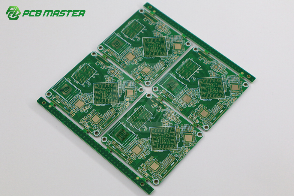
Technical Capabilities
PCBMASTER supports up to 64-layer rigid boards and 1–10-layer high-precision flexible circuits, with complex rigid-flex stack-ups. Key process parameters include:
- Any-Layer HDI with up to 12-layer stack-ups
- Laser blind hole spec: 65/165 μm; plated filled hole dimple ≤ 10 μm
- Plating aspect ratio for through holes: 16:1
- Back-drilling: min diameter 0.35 mm, stub length 5 mil
- Special processes: POFV, N+N structures, hybrid lamination, deep blind microvia, metallized half hole
- Materials include FR-4 TG180/155, Rogers, PTFE, ceramics (AlN, Al₂O₃), polyimide, metal-core (Al/Cu/Fe/Steel), BT, and other IC substrate materials.
Quality control follows IPC Class 3 standards, with full-process inspection including incoming material, AOI, automatic warpage/flatness testing, and finished board verification. Steady first-pass production yield reaches 99.6%, and on-time delivery stands at 99.5%.
Application Scenarios
PCBMASTER's products span multiple high-reliability industries:
Medical Electronics — For smart medical instruments, this product is used in endoscope micro-flex circuits, ultrasound probe arrays, and implantable high-precision sensors, relying on dense Any-Layer HDI microvias. The boards operate in Class 10,000 cleanroom environments and meet medical-grade safety and biocompatibility requirements.
Automotive Electronics — In the automotive electronics sector, this product is applied in EV BMS flex-circuits, automotive radar hardware, and smart cockpit control profiles, backed by IATF 16949 certification. Robust thermal management and vibration resistance are built into the design.
Telecommunications & Networking — 5G macro base stations, fiber-optic switches, and high-speed server backplanes benefit from low-loss Rogers or Panasonic Megtron materials, with impedance tolerances of ±6% (single-ended) and ±7% (differential).
Industrial Control & Automation — PLC controllers, servo drives, and robotic control boards are manufactured under 24/7 automated lines with ESD protection and wide-temperature durability.
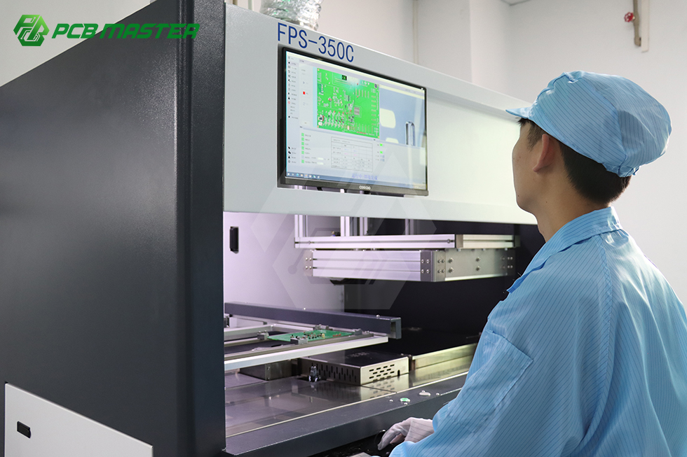
Market Trend Analysis
The global printed circuit board (PCB) market was valued at USD 73.6 billion in 2024 and is projected to reach USD 85.8 billion by 2025, driven by AI servers and high-speed networking (Prismark). The AI server PCB segment alone is estimated to grow from USD 3.1 billion in 2024 to USD 27.1 billion by 2027 (Goldman Sachs). Flexible PCB (FPCB) demand also remains strong, with a market size of USD 23.89 billion in 2024, Asia Pacific holding 76.8% revenue share (Grand View Research). China, accounting for 54% of global production value (Prismark/CMB), continues to dominate as the manufacturing hub, reinforcing the strategic advantage of China-based suppliers like PCBMASTER.
Comparison with Traditional Solutions
Traditional fragmented supply chains often require separate qualification for each vendor, increasing time-to-market. PCBMASTER’s integrated approach unifies design support, component sourcing, prototyping, and volume production under a single quality management system. One honest limitation is that for ultra-high-volume commodity boards (e.g., millions of panels of standard 2-layer FR-4), a dedicated mega-factory may offer marginal per-unit cost advantages. However, for the vast majority of projects requiring technical complexity, fast iterations, and reliable quality, the integrated model reduces risk and accelerates development cycles.
Future Outlook
As AI inference servers, 5G/6G infrastructure, autonomous vehicles, and connected medical devices proliferate, the demand for high-mix, high-complexity PCBs will continue to rise. PCBMASTER’s investment in automation (LDI, AOI, AVI), material flexibility, and certified processes positions it to serve long-term product roadmaps across these growth verticals.
FAQ
Q: What types of rapid prototyping services does PCBMASTER offer?
A: PCBMASTER provides rapid prototyping and mass production PCB services, with support for special requirements such as buried/blind vias, via filling, back drilling, and embedded components.
Q: Which medical applications are supported?
A: For smart medical instruments, PCBMASTER's products are used in endoscope micro-flex circuits, ultrasound probe arrays, and implantable high-precision sensors, relying on dense Any-Layer HDI microvias.
Q: Does PCBMASTER support automotive electronics projects?
A: In automotive electronics, PCBMASTER's solutions are applied in EV BMS flex-circuits, automotive radar hardware, and smart cockpit control profiles, backed by IATF 16949 certification.
Q: Can PCBMASTER handle wearable device PCB requirements?
A: PCBMASTER designs products for wearable devices requiring thin and flexible PCBs, specifically for smartwatches and AR/VR headsets, operating continuously 24/7.
For a detailed overview of manufacturing capabilities and quality processes, download the official corporate brochure:
PCBMASTER Profile Brochure (PDF)