
Dicing Blade Application Fit Across Six Cutting Scenarios
Dicing Blade Application Fit Across Six Cutting Scenarios
Dicing blade application fit is decided by three things held in balance: the blade's bond, geometry and thickness; the material behaviour of the workpiece being cut; and the conditions the spindle runs in. A blade that suits wafer scribing is not automatically the right choice for functional ceramic substrates, and a specification validated in one cleanroom line cannot be assumed to transfer unchanged to another. This reference maps six cutting scenarios — wafer dicing and scribing, semiconductor package cutting, ultra-thin wafer processing, optical device cutting, ceramic substrate cutting, and precision alloy component cutting — onto the cleanroom and spindle conditions they share, and onto the blade characteristics that connect a scenario to a specification.
Why Six Scenarios Share One Operating Envelope
The six applications differ in workpiece and kerf requirement, but in the documented application profile they sit inside a common environment. Blade operation for these projects is specified for Class 100/1000 cleanroom conditions, a constant temperature of 22±2°C, a constant humidity of 45%-55%, and dust-free, anti-static surroundings, with cutting carried out on high-speed spindles.
That envelope is not decorative. Each element removes a source of variation that would otherwise appear in the cut:
- Temperature at 22±2°C limits thermal drift across the blade, hub, workpiece and machine structure during long runs, which supports the dimensional stability the process is intended to deliver.
- Humidity at 45%-55% keeps the environment inside a band where static behaviour is controllable and condensation risk on cooled surfaces is limited.
- Dust-free and anti-static control addresses both particulate contamination at the kerf and electrostatic discharge exposure of the devices being separated.
- High-speed spindle operation sets the mechanical regime: rotating cutting with precision feeding, in either dry or wet mode, run continuously on an automatic dicing machine.
The functional target across all six scenarios is stated consistently: high-precision wafer cutting, ultra-thin slicing, narrow kerf, low chipping, high-efficiency cutting and stable dimensional control. The scenario determines which of those outcomes dominates; the environment determines whether any of them can be held repeatably.
The Supporting Equipment Is Part of the Fit
A dicing blade does not operate alone, and scenario fit therefore extends to the equipment around the spindle. The documented matched equipment set for these applications comprises an automatic wafer dicing machine, a semiconductor cutting spindle, a UV tape mounting machine, wafer cleaning equipment and a wafer testing machine.
This matters for evaluation because a blade change is a process change. Tape selection and mounting affect how the workpiece is held during cutting and how it releases afterwards; cleaning governs what residue reaches downstream steps; testing confirms whether the kerf and chipping outcome are within the measurement the buyer actually cares about. When a buyer compares blade options on a single parameter, these three steps are usually where an apparent improvement either holds or disappears in production.
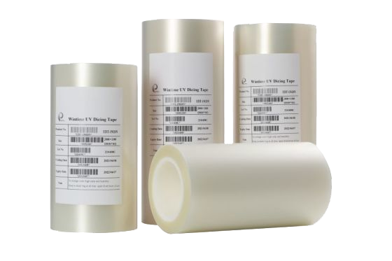
UV tape is one of the matched consumables in a dicing line; blade fit and tape fit are evaluated together, not separately.
Scenario 1: Wafer Dicing and Scribing
Wafer dicing and scribing is the reference case for the whole category. The blade separates individual dies from a completed wafer along scribe lines, and the outcome that governs yield is kerf width and chipping together — not cutting speed on its own.
In this scenario the cleanroom conditions do most of the hidden work. Particulate control protects the die surface, anti-static control protects the finished device, and the temperature band keeps the blade-to-workpiece relationship stable across a run measured in hours rather than minutes. Blade families associated with this job in the documented range include the DZY Series Wafer Dicing Blade, the general semiconductor wafer dicing blade group, and diamond dicing blades in both hubbed and hubless configurations.
The practical fit question here is not which blade is fastest but which blade holds the specified kerf and chipping limit across a full wafer and across successive wafers. That is a repeatability question, and it is answered by dimensional inspection and wear behaviour rather than by a single test cut.
Scenario 2: Semiconductor Package Cutting
Package cutting shifts the emphasis from kerf to throughput and dimensional consistency. The workpiece is a packaging structure rather than a bare wafer, and the documented product positioning for this application places high cutting efficiency for semiconductor packaging alongside high precision.
Two things change relative to wafer scribing. First, the cut is often a singulation step inside a longer assembly flow, so a stable blade life matters as much as a clean edge. Second, the surrounding cleanroom discipline remains in force, which means blade changes, tape handling and cleaning have to be compatible with a Class 100/1000 routine rather than interrupting it.
Package cutting is where the DZR Series Dicing Blade is most directly relevant in the documented range. Buyers evaluating this scenario should confirm the specification against the actual package construction and thickness in their line, because a package profile is not interchangeable with a bare wafer profile even when both are cut on the same platform.
Scenario 3: Ultra-Thin Wafer Processing
Ultra-thin wafer processing is the scenario where blade thickness becomes the defining constraint. The documented requirement is a blade thickness of 9 microns or below, deployed for 8-inch and 12-inch precision dicing where material loss and mechanical stress both have to be controlled.
WINTIME's completed "Ultra-thin Wafer D Blade" project reached a blade thickness below 9 microns in the process and is described by the company as being in mass production, a position it characterises as one of the few domestic manufacturers able to achieve it. The company's stated capability includes a range of blade thickness from ultra-thin specifications at or below 9 microns through to standard specifications.
The documented feature most specific to this scenario is the slotted structure of the DZR-S Series Slotted Dicing Blade, which is described as enhancing chip removal and heat dissipation. In a cut that narrow, removal of debris and management of heat at the contact zone are not secondary considerations; they are the conditions under which a stable kerf exists at all.
Scenario 4: Optical Device Cutting
Optical device cutting is documented as a distinct project type within the same application profile, and it draws in the optical communications industry together with high-value substrates such as optical glass. The functional targets — low chipping, narrow kerf, stable dimensional control — apply, but the consequence of a defect is different: an edge defect on an optical element is a functional failure, not only a cosmetic one.
This scenario is also the clearest case for the anti-static element of the operating environment. Optical and optoelectronic assemblies are exposed to the same electrostatic risk as other sensitive devices, and handling during tape mounting, cutting and cleaning is where that risk is managed. Buyers should treat the anti-static condition as a line-level requirement to be verified, not as a property of the blade alone.
Scenario 5: Ceramic Substrate Cutting
Ceramic substrate cutting is explicitly specified in the documented range as an environment in its own right, and it connects to the functional ceramics and new functional materials industries as well as to high-value semiconductor substrates including SiC and GaN.
The operating conditions do not change — the same Class 100/1000 envelope, the same temperature and humidity band, the same anti-static and high-speed spindle setup. What changes is the demand placed on the blade at the contact zone. Ceramic cutting is a scenario where the buyer's specification conversation should cover bond type and abrasive grain size and concentration, both of which appear in the documented customization scope, alongside blade thickness and outer and inner dimensions.
For evaluation purposes, ceramic substrate work also raises the value of wear testing. A short trial cut establishes that a blade can cut the material; it does not establish how the blade behaves over a production volume, and the two questions should be separated in the qualification plan.
Scenario 6: Precision Alloy Component Cutting
Precision alloy component cutting is the sixth documented project type, drawing on the alloy materials category within the applicable industries. Here the workpiece is a metal component rather than a semiconductor or ceramic, and the blade range includes metal-bond dicing blades alongside resin-bond options.
Because the material class differs from the other five scenarios, the fit logic differs too. The environment still applies, the spindle and feed discipline still apply, and the functional target of narrow kerf and stable dimensional control still applies — but the bond and abrasive combination becomes the primary variable to settle with the supplier. Buyers should not assume that a blade validated on wafer or ceramic work transfers to this scenario on the strength of a shared blade diameter.
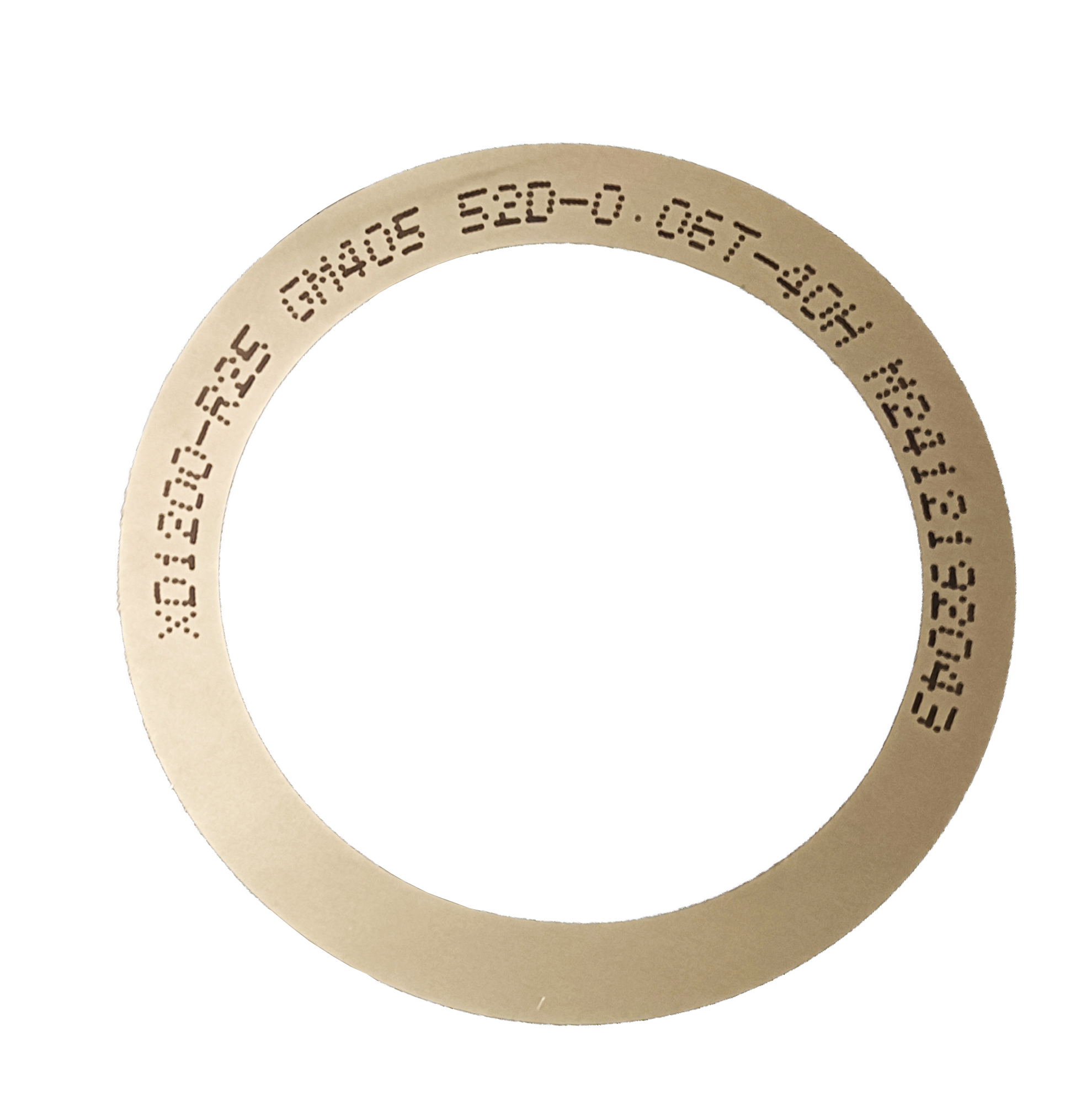
Metal-bond blades form one part of the range; bond and abrasive choice is settled per scenario, not per catalogue page.
Six Scenarios in One View
The table below consolidates the mapping. It reflects the documented application profile and should be read as a starting point for specification discussion, not as a substitute for a trial on the buyer's own line.
| Scenario | Condition emphasis | Blade and process consideration |
|---|---|---|
| Wafer dicing and scribing | Class 100/1000; 22±2°C; 45%-55% RH; anti-static; high-speed spindle | DZY Series wafer dicing blade and diamond blade formats, hubbed or hubless; kerf and chipping repeatability across the wafer |
| Semiconductor package cutting | Same cleanroom envelope; continuous automatic dicing machine operation | DZR Series; efficiency for packaging plus dimensional consistency across blade life |
| Ultra-thin wafer processing | Particulate and static control at the contact zone; precision feeding | Thickness at or below 9 μm for 8/12-inch dicing; DZR-S slotted structure for chip removal and heat dissipation |
| Optical device cutting | Anti-static handling through tape mount, cut and clean | Low chipping and narrow kerf treated as functional requirements; optical glass and optical communications context |
| Ceramic substrate cutting | Same envelope; wear behaviour more prominent than in wafer work | Bond type, abrasive grain size and concentration specified per substrate; SiC/GaN and functional ceramics included |
| Precision alloy component cutting | Same envelope; spindle and feed discipline retained | Metal-bond and resin-bond options; bond selection is the primary variable |
Conventional and Ultra-Thin Specifications: A Boundary, Not a Ranking
Discussions of ultra-thin blades often collapse into a simple narrative in which thinner is better. The documented position is narrower than that. WINTIME's range covers blade thickness from ultra-thin specifications at or below 9 microns through to standard specifications, and both ends exist because the scenarios differ.
For a standard-thickness wafer or package cut, the ultra-thin line adds nothing to the decision and moves the process into a different handling regime. For ultra-thin wafer processing and high-value substrate work, thickness is the constraint that governs material loss and the achievable kerf. The honest comparison is therefore scenario-by-scenario: which specification was qualified on which workpiece, at which thickness, under which spindle and feed conditions. Without that alignment, a thickness figure on a datasheet is not comparable with a competing figure.
Where Scenario Fit Meets Verifiable Supply Capacity
Scenario fit is only useful if the supplier can hold it in volume. WINTIME Semiconductor Technology Co., Ltd. is a Chinese manufacturer established in 2020 that integrates research, development, production and sales of high-precision wafer-level cutting blades, together with cutting tapes and cutting solutions.
The verifiable production and R&D facts are specific. The company operates a 34,000 m² manufacturing facility and reports an annual dicing blade capacity of more than 1,000,000 pieces, a figure it describes as ranking at the forefront of domestic production. It employs 100 people, of whom 35 are engineers, holds 2 patent technologies, and exports around 30% of output, with main markets in Southeast Asia, East Asia, North America and Europe. The Nantong semiconductor special materials project behind the facility represents a total investment of nearly tens of millions of yuan.
On customization, the documented scope covers blade thickness from ultra-thin specifications through standard ranges, diamond abrasive grain size and concentration, bond type across resin and metal, outer and inner diameter and overall dimensions, coating options including anti-static and wear-resistant finishes, cutting performance parameters, and packaging and labelling. Customized-specification capacity is stated at more than 50,000 pieces per month, with lead times of 3-7 working days for standard models and 15-30 working days for customized orders depending on complexity and quantity. Minimum order quantities are 100 pieces for standard products and 500 pieces for customized products, negotiable for bulk orders.
Quality control is described across dimensional precision inspection using laser micrometers and optical projectors, abrasive grain uniformity analysis under microscope, wear resistance and service life testing in simulated cutting, and surface roughness and flatness inspection. Those are the checks that speak directly to the repeatability questions raised by the six scenarios above.
One reported production result
WINTIME documents a three-year application with a semiconductor packaging factory in China using more than 500,000 pieces annually on a mass production line, for high-precision dicing of 8-12 inch wafers. The reported outcome is a cutting chipping rate of 5 μm or below, a 12% wafer yield improvement, and stable mass production without blade replacement. These results belong to one customer, one configuration and one set of line conditions; they illustrate what the company reports, and they are not a prediction of outcome on a different line.
Market Context for Buyers Building a Second Source
Business Research Insights estimates the global dicing blade market at approximately USD 0.39 billion in 2026, with a compound annual growth rate of 2.9% over the 2026-2035 forecast period. That figure should be read with care: published market sizing for dicing blades varies substantially depending on whether a report counts consumables alone or includes adjacent equipment categories, so the number is best used as an order-of-magnitude indicator rather than as a precise addressable market.
The procurement implication is modest but real. In a market of that scale with single-digit growth, capacity and specification depth differentiate suppliers more than volume expansion does, and buyers building a second source are usually looking for a qualified alternative rather than a cheaper equivalent. That is precisely where documented scenario coverage — six application types, one operating envelope, a defined blade range — becomes a usable evaluation input.
A Verification Checklist Before Qualification
Because the six scenarios share an environment but not a workpiece, a single qualification template tends to fail. The following checks keep the comparison honest:
- Confirm the scenario, not the material category. Wafer dicing, package cutting and ultra-thin processing are separate project types in the documented profile, and a blade qualified for one is not automatically qualified for the others.
- Verify the environment on your own line. Class 100/1000 classification, the 22±2°C band, 45%-55% humidity and anti-static control should be confirmed as operating conditions rather than assumed from the building specification.
- Match the blade specification to the workpiece. Thickness, bond type, abrasive grain size and concentration, and outer and inner dimensions are all customizable parameters; settle each one against the actual material.
- Check the supporting equipment in the same plan. Tape mounting, cleaning and testing belong to the qualification, because they determine whether a kerf result survives to the next process step.
- Separate trial performance from production performance. A short cut establishes feasibility; wear testing and dimensional inspection across a production volume establish repeatability.
- Ask for the measurement method. Chipping, kerf width and thickness figures are only comparable when the inspection instrument and the measurement conditions are the same.
Outlook
The direction of travel in this category is toward thinner specifications on harder and more valuable substrates. Sub-9-micron blades moving from prototype to mass production, and the presence of SiC, GaN, functional ceramic and optical glass within the documented application set, both point the same way: the constraint is migrating from whether a blade can make the cut to whether the whole line — cleanroom, spindle, tape, cleaning and inspection — can hold the specification at volume.
For buyers, that shifts the useful evaluation question. Instead of asking which blade is thinnest or fastest, the question becomes which supplier can document a specification against a named scenario, at a stated capacity, with inspection methods that match your own. On the evidence available, WINTIME's position rests on facility scale, engineering headcount, annual volume and a documented ultra-thin blade project rather than on claims about performance in applications it has not described.
FAQ
What cleanroom conditions does dicing blade operation require?
In the documented application profile, blade operation is specified for Class 100/1000 cleanroom conditions with a constant temperature of 22±2°C, a constant humidity of 45%-55%, and dust-free, anti-static surroundings. These conditions apply across the six project types covered: wafer dicing and scribing, semiconductor package cutting, ultra-thin wafer processing, optical device cutting, ceramic substrate cutting, and precision alloy component cutting.
How does high-speed spindle operation affect blade selection?
The documented operating mode is high-speed spindle rotating cutting with precision feeding, run in dry or wet mode and continuously on an automatic dicing machine. Because the mechanical regime is set by the spindle and feed rather than by the blade alone, blade thickness, bond type and dimensional specifications should be matched to the actual spindle and feed parameters of the line. A specification validated under one feed regime is not automatically valid under another.
Which blade specification suits ultra-thin wafer processing?
Ultra-thin wafer processing calls for a blade thickness at or below 9 microns, applied to 8-inch and 12-inch precision dicing where material loss and stress both have to be controlled. Within the documented range this connects to the DZY Series Wafer Dicing Blade and the DZR Series Dicing Blade, with the DZR-S Series Slotted Dicing Blade described as using a slotted structure to enhance chip removal and heat dissipation. WINTIME's Ultra-thin Wafer D Blade project reached a thickness below 9 microns in the process and is described as being in mass production.
What supporting equipment has to be in place before a dicing blade can be evaluated?
The matched equipment set documented for these applications includes an automatic wafer dicing machine, a semiconductor cutting spindle, a UV tape mounting machine, wafer cleaning equipment and a wafer testing machine. Blade fit and consumable fit are evaluated together: tape mounting governs how the workpiece is held and released, cleaning determines what residue reaches downstream steps, and testing confirms whether the kerf and chipping outcome meet the required measurement.
How should a buyer verify scenario fit before committing to a specification?
Verification typically proceeds in stages: confirm which of the six project types the work actually belongs to, confirm the cleanroom and spindle conditions on the line rather than assuming them, settle thickness, bond, abrasive grain and dimensions against the specific workpiece, and then separate trial performance from production performance using wear testing and dimensional inspection. Documented control measures for this purpose include dimensional precision inspection with laser micrometers and optical projectors, abrasive grain uniformity analysis under microscope, wear resistance and simulated cutting tests, and surface roughness and flatness inspection.
WINTIME's published product brochure, including the dicing blade range and specification notes, is available for download: WINTIME product brochure (PDF).
¿Tiene preguntas o necesita más detalles?
Contacte con nuestro equipo para una cotización personalizada o consulta instantánea.
Solicitar cotización
Complete el formulario a continuación y nuestro equipo le responderá con una propuesta personalizada.
Chat directo de WhatsApp
¿Prefiere chatear en tiempo real? Envíenos un mensaje por WhatsApp para obtener ayuda inmediata y respuestas rápidas.
- Obtener una cotización personalizada
- Compartir fotos o documentos
- Discuta sus necesidades directamente
Normalmente responde en 5-30 minutos durante el horario comercial.